In our increasingly interconnected and technology-driven world, we often marvel at the lightning speed of our smartphones, the intricate power of supercomputers, and the breathtaking clarity of modern displays. Yet, beneath the polished surfaces and sleek designs lies a fundamental principle, often unseen but incredibly vital, that propels these innovations forward: mobility in physics. Far from merely describing the ability to move, this concept, when understood through the lens of physics, represents a critical metric dictating the very efficiency and performance of electronic components. It is the silent architect behind the relentless march of technological progress, constantly being optimized and redefined by brilliant minds across the globe.
Imagine the intricate dance of tiny charge carriers – electrons and holes – as they navigate the complex landscape of a semiconductor material. Their ability to respond swiftly and efficiently to an electric field isn’t just a matter of speed; it’s a profound determinant of how quickly your processor executes commands, how brightly your LED shines, and how effectively your solar panel converts sunlight into energy. This intrinsic property, meticulously studied and engineered, fundamentally shapes the capabilities of every digital device we interact with daily. Understanding its nuances is not merely an academic exercise; it’s an exploration into the very bedrock of our electronic future.
| Concept | Description |
| Definition | A measure of how easily charge carriers (electrons or holes) move through a material under the influence of an electric field. It quantifies their responsiveness to electrical forces, determining how efficiently current flows. |
| Key Formula | μ = vd / E, where μ is mobility, vd is drift velocity (the average velocity of charge carriers in an electric field), and E is the applied electric field. |
| Units | Typically measured in square centimeters per volt-second (cm²/(V·s)). Higher values indicate greater ease of movement. |
| Factors Affecting Mobility | Temperature (increased thermal vibrations hinder movement), impurity concentration (scattering events), material type and crystal structure, defects, and the effective mass of the charge carriers. |
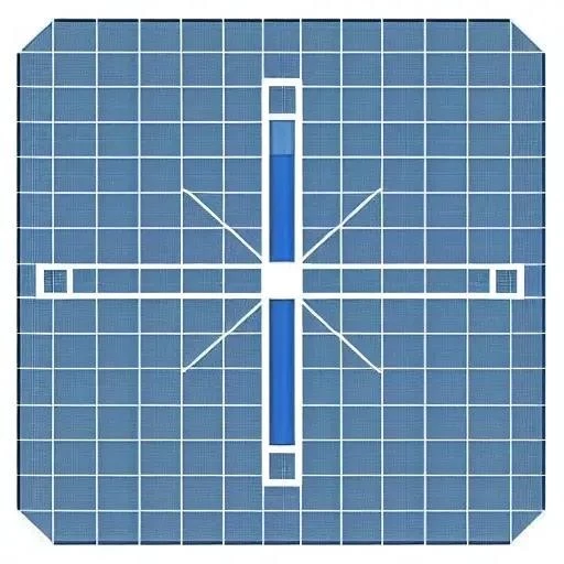
| Primary Application Area | Semiconductor physics and engineering, crucial for the design, optimization, and performance of transistors, diodes, integrated circuits, solar cells, and LEDs. |
| Impact on Technology | Higher charge carrier mobility directly translates to faster switching speeds, lower power consumption, reduced heat generation, and improved overall efficiency in electronic devices. |
| Reference (General) | Wikipedia: Electron Mobility |
At its core, charge carrier mobility (μ) is the proportionality constant between the drift velocity (vd) of a charge carrier and the applied electric field (E). Imagine a race car, meticulously engineered, on a perfectly smooth track; its mobility would be exceptionally high, allowing it to accelerate and maintain speed with minimal resistance. Conversely, a car on a bumpy, crowded road would exhibit low mobility, struggling to gain momentum. In the microscopic world of materials, electrons and holes are these “race cars,” and the crystal lattice, with its atoms, impurities, and defects, constitutes the “track.” Higher mobility signifies fewer collisions and less scattering, permitting charge carriers to traverse the material more freely and thus conduct electricity more efficiently. This fundamental understanding is driving unprecedented advancements in material science.
The practical implications of optimizing mobility are staggeringly significant, particularly within the semiconductor industry. For decades, Silicon Valley’s titans have been engaged in a relentless pursuit of higher mobility, knowing that every incremental improvement directly translates into faster transistors, more powerful microprocessors, and ultimately, more advanced technology for consumers. Consider the transformative impact on data centers, where even a slight increase in processor efficiency, directly linked to mobility, can lead to substantial energy savings and computational gains. Groundbreaking research into novel materials like graphene and other two-dimensional semiconductors, boasting mobilities orders of magnitude higher than silicon, promises a future where devices are not only faster but also consume dramatically less power, effectively pushing the boundaries of what’s currently conceivable.
Looking ahead, the journey to unlock the full potential of mobility is incredibly exciting. Researchers worldwide are leveraging sophisticated AI and machine learning algorithms to predict and synthesize new materials with optimized electronic properties, accelerating discovery cycles that once took years. By integrating insights from advanced computational models, scientists are designing novel semiconductor structures that minimize scattering events, thereby boosting carrier mobility to unprecedented levels. This forward-thinking approach is not just about incremental gains; it’s about fundamentally rethinking material design from the atomic level upwards. The persistent pursuit of enhanced mobility promises to usher in an era of truly revolutionary devices, powering everything from ultra-efficient quantum computers to seamlessly integrated augmented reality experiences, shaping a future that is not only smarter but also more sustainable. The journey of these unseen particles continues to redefine our technological horizon.